1920 × 1080
12.8-inch TFT LCD with a 283.39 × 159.41 mm active area.
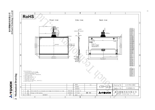
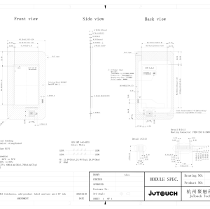
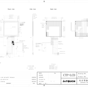
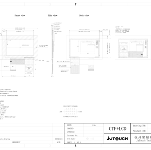
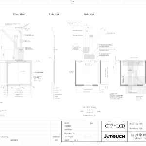
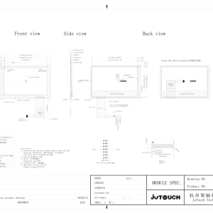
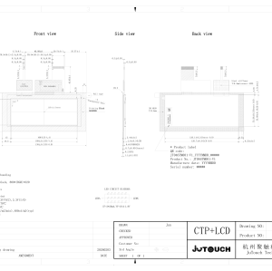
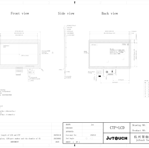
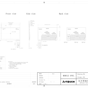
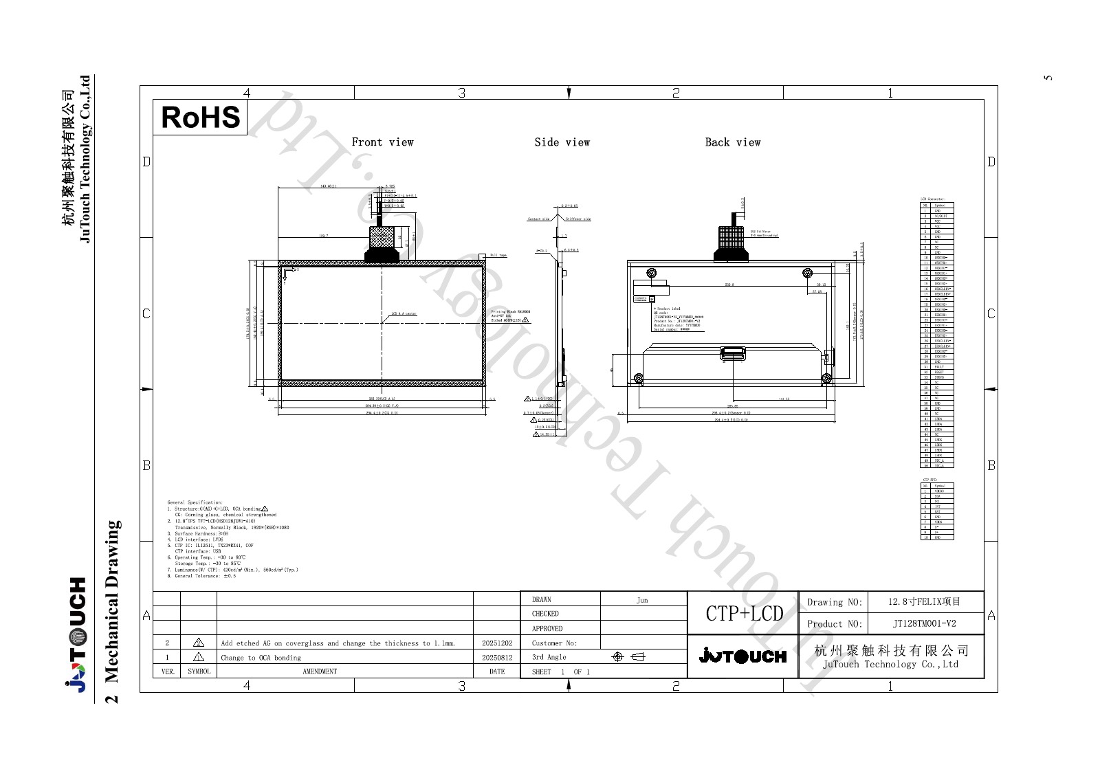
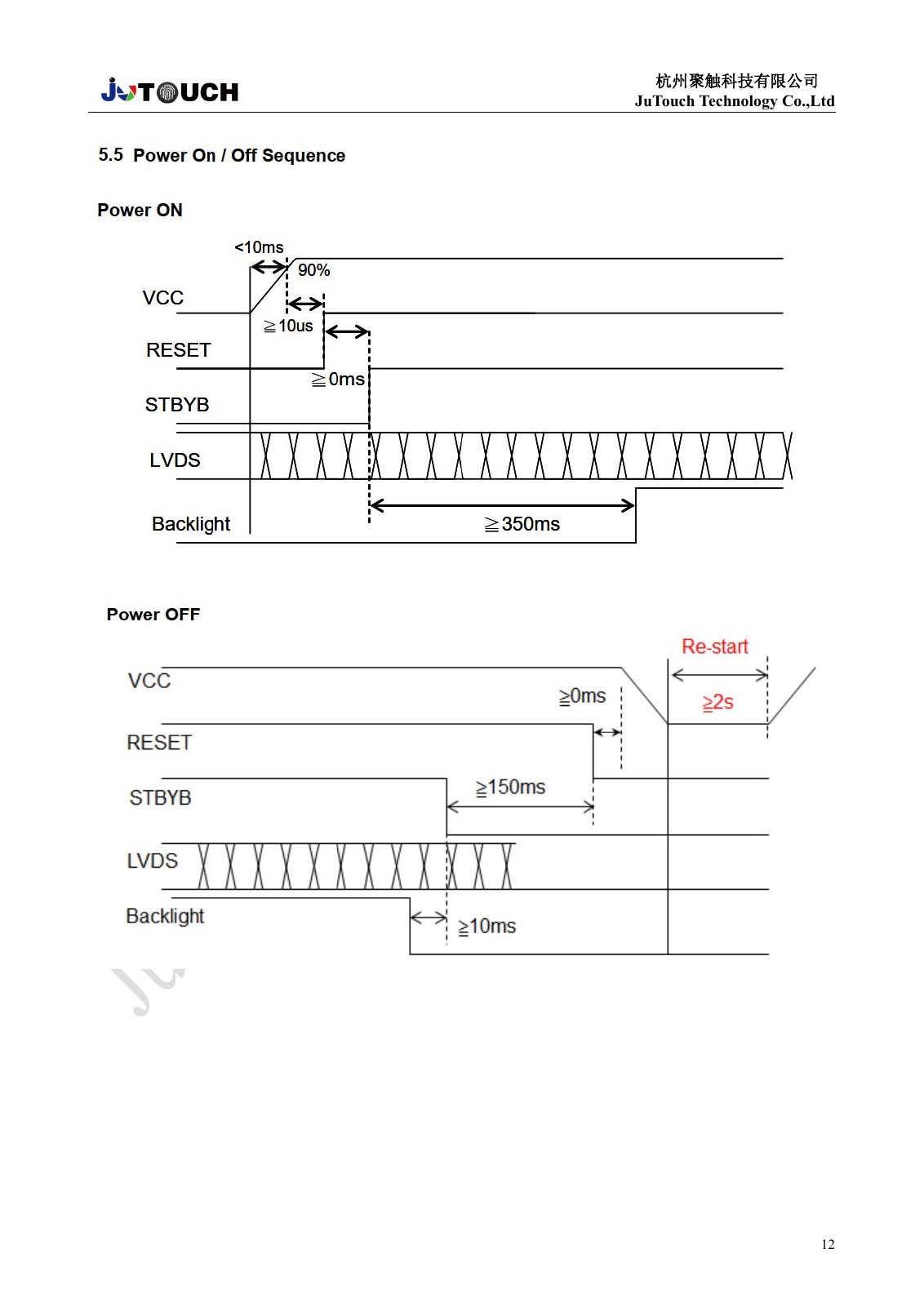
JT128TM001-V2 is a 12.8-inch CTP + LCD module with 1920 × 1080 resolution, LVDS video and USB / I2C touch interfaces. It combines a G+G touch structure with optical bonding, an ILI2511 controller, 10 touch points and an etched anti-glare surface. This page is based on the preliminary specification dated January 12, 2026. Optical-table luminance is 560 nits typical with CTP. The mechanical drawing separately lists 800 nits; this discrepancy requires confirmation before design approval. No 800-nit or sunlight-readable claim is made here. 12.8-inch TFT LCD with a 283.39 × 159.41 mm active area. G+G+LCD structure, etched AG surface and 6H hardness. ILI2511 controller; USB / I2C touch interfaces. Outline dimensions: 294.4 × 178.5 × 14.25 mm, excluding PCBA. View the full-size drawing. 50-pin FPC connector: AORORA F31L-1A7H1-21050 or BJD 101049-205050, as named in the source. NTC: Murata NCU15XH103F6SRC. These are source-listed limits, not nominal supply settings. The horizontal-display timing is for two-port LVDS; it does not change the 1920 × 1080 panel resolution. Follow the source sequence for VCC, RESET, STBYB, LVDS and backlight. The diagram lists a restart interval of at least 2 seconds. The source lifetime table and its notes use different current conditions. No lifetime claim is made until these are reconciled. The source specifies a 12S4P, 48-LED circuit and recommends constant-current drive. Review the full backlight thermal/current requirements before integration. “—” means not specified; TBD values remain unresolved. Source measurement guidance specifies 30-minute stabilization and 30-minute backlight warm-up in a windless room. White uniformity is minimum divided by maximum luminance across nine points, multiplied by 100%. These are specification test conditions, not independent certification or proof of completed qualification. The source requires no surface condensation during testing, a maximum display-surface temperature of 85°C and at least 24 hours of recovery at room temperature before cosmetic/function inspection. Confirm the preliminary specification revision, brightness discrepancy, backlight current/lifetime conditions, mechanical fit and host LVDS compatibility before sample approval. Supply the model number, required quantity, host details and enclosure drawing when making an inquiry.12.8-Inch Optical Bonded Capacitive Touch Display
Key Features
1920 × 1080
Optical Bonding
10-Point Touch
Original Mechanical Drawing
General Specifications
Parameter Specification Module size 12.8 inches Structure G+G+LCD; optical bonding Resolution 1920(RGB) × 1080 Display mode Normally black, transmissive Pixel pitch 0.1476(W) × 0.1476(H) mm Pixel arrangement RGB stripe Viewing direction ALL O’clock Outline 294.4(W) × 178.5(H) × 14.25(D) mm; W/O PCBA Active area 283.39(W) × 159.41(H) mm LCD interface LVDS CTP interface USB / I2C CTP controller ILI2511 Touch points 10 Surface hardness 6H Surface treatment Etched AG LCD Pin Assignment — CN1
Pin Symbol Description 1 GND Power ground 2 NC/BIST No connector (BIST pin) 3 VCC Digital power / Vin = 3.3 V 4 VCC Digital power / Vin = 3.3 V 5 GND Power ground 6 GND Power ground 7 NC No connector 8 NC No connector 9 GND Power ground 10 ORXIN0- LVDS differential input: Negative odd data 0 11 ORXIN0+ LVDS differential input: Positive odd data 0 12 ORXIN1- LVDS differential input: Negative odd data 1 13 ORXIN1+ LVDS differential input: Positive odd data 1 14 ORXIN2- LVDS differential input: Negative odd data 2 15 ORXIN2+ LVDS differential input: Positive odd data 2 16 ORXCLKIN- LVDS differential input: Negative odd clock 17 ORXCLKIN+ LVDS differential input: Positive odd clock 18 ORXIN3- LVDS differential input: Negative odd data 3 19 ORXIN3+ LVDS differential input: Positive odd data 3 20 ERXIN0- LVDS differential input: Negative even data 0 21 ERXIN0+ LVDS differential input: Positive even data 0 22 ERXIN1- LVDS differential input: Negative even data 1 23 ERXIN1+ LVDS differential input: Positive even data 1 24 ERXIN2- LVDS differential input: Negative even data 2 25 ERXIN2+ LVDS differential input: Positive even data 2 26 ERXCLKIN- LVDS differential input: Negative even clock 27 ERXCLKIN+ LVDS differential input: Positive even clock 28 ERXIN3- LVDS differential input: Negative even data 3 29 ERXIN3+ LVDS differential input: Positive even data 3 30 GND Power ground 31 FAULT Normal = L; abnormal = H 32 RESET Global reset, active low 33 STBYB Standby mode, active low 34 NC No connector (serial chip enable CSB) 35 NC No connector (serial clock SCL) 36 NC No connector (serial data CDA) 37 NC No connector (serial data CDA) 38 GND Power ground 39 GND Power ground 40 NC No connector 41 LEDA LED power (anode) 42 LEDA LED power (anode) 43 LEDA LED power (anode) 44 NC No connector 45 LEDK Cathode 1 46 LEDK Cathode 2 47 LEDK Cathode 3 48 LEDK Cathode 4 49 NTC_A NTC anode 50 NTC_K NTC cathode CTP Pin Assignment
Pin Symbol Description 1 VDD33 I2C power supply: 3.3 V 2 SDA I2C data 3 SCL I2C clock 4 INT I2C interrupt 5 RST Reset, active low 6 GND Power ground 7 VDD5 USB power supply: 5 V 8 D- USB data minus 9 D+ USB data plus 10 GND Power ground Absolute Maximum Ratings
Parameter Symbol Min. Max. Unit Power supply VCC -0.3 4 V Operating temperature TOP -30 +85 °C Storage temperature TST -40 +90 °C LCD Electrical Characteristics
Item Symbol Min. Typ. Max. Unit Condition Supply voltage VCC 3 3.3 3.6 V — Input high ViH VCC × 0.7 — VCC V — Input low ViL 0 — VCC × 0.3 V — Supply current IDD — — 500 mA VCC=3.3 V, white pattern Inrush current IRUSH — — 2.0 A Source test circuit; 2 ms rising time LVDS Receiver Characteristics
Item Symbol Min. Typ. Max. Unit Condition Differential high threshold Vth — — 100 mV VCM=1.2 V Differential low threshold Vtl -100 — — mV VCM=1.2 V Input current IIN -10 — +10 µA — Differential input voltage |VID| 0.1 — 0.6 V — Common-mode voltage offset VCM 1 1.2 1.7 − (|VID| / 2) V — Two-Port LVDS Timing — DE Mode
Item Symbol Min. Typ. Max. Unit Frame rate FR 55 60 65 Hz Vertical display time Tvd — 1080 — H Vertical pulse width Tvpw 1 3 20 H Vertical back porch Tvbp 2 24 200 H Vertical front porch Tvfp 5 8 200 H Frame period Tv 1087 1112 1404 H Horizontal display time Thd — 960 — DCLK Horizontal pulse width Thpw 10 12 200 DCLK Horizontal back porch Thbp 5 16 200 DCLK Horizontal front porch Thfp 24 26 200 DCLK One horizontal line Tv (source label) 989 1012 1248 DCLK Clock rate FDCLK 64.5 66.9 80 MHz 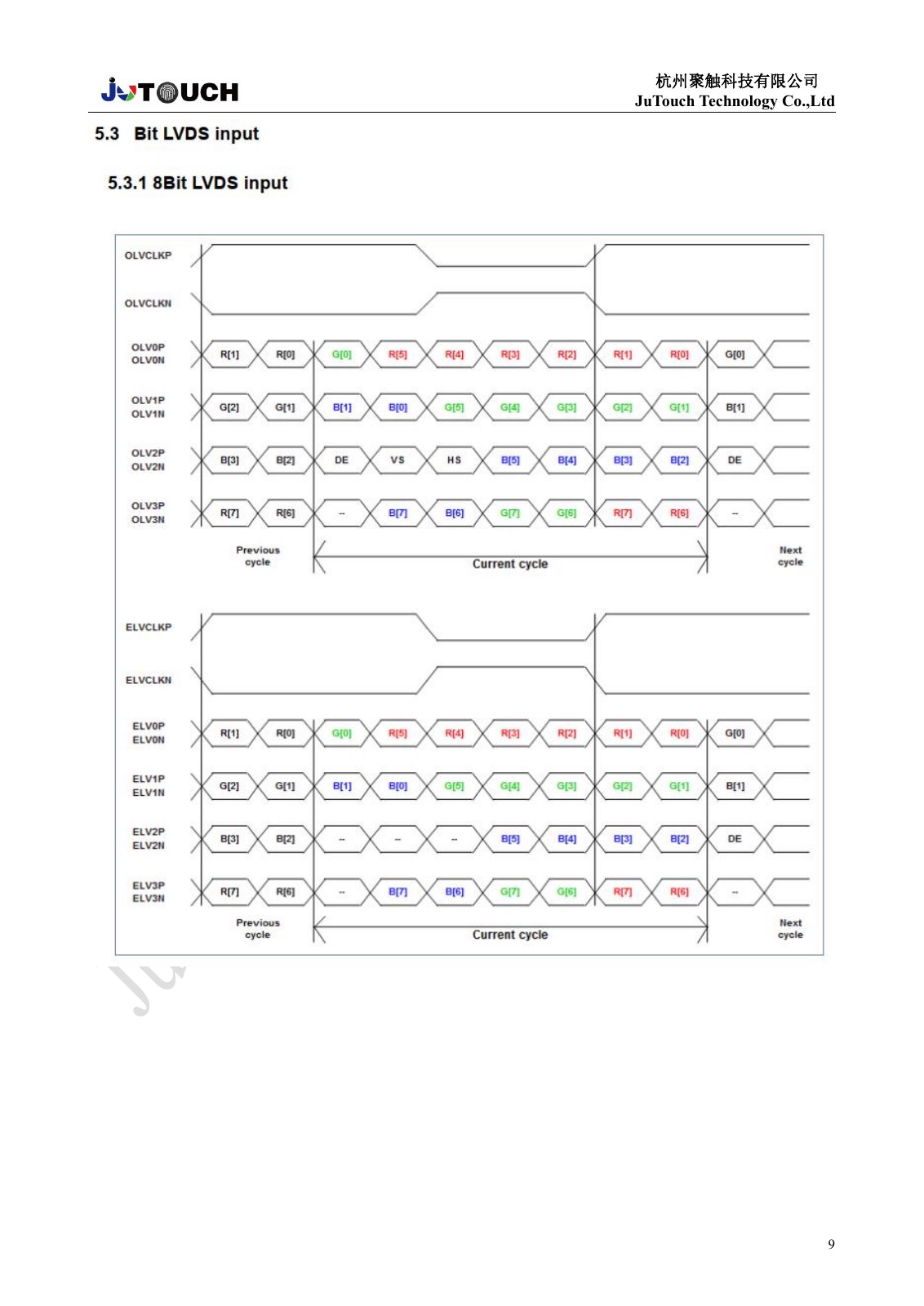
Power-On / Power-Off Sequence
Backlight Parameters
Parameter Symbol Min. Typ. Max. Unit Source condition LED current IF — 340 — mA Ta=25°C LED voltage VF — 38.4 40.8 V Ta=25°C Optical Characteristics
Item Condition Min. Typ. Max. Unit Viewing angle: Horizontal θx+ CR ≥ 10 80 85 — degrees Viewing angle: Horizontal θx- CR ≥ 10 80 85 — degrees Viewing angle: Vertical θy+ CR ≥ 10 80 85 — degrees Viewing angle: Vertical θy- CR ≥ 10 80 85 — degrees Luminance with CTP θx=0°, θy=0° 420 560 — nit 9-point uniformity θx=0°, θy=0° 70 80 — % Contrast ratio θx=0°, θy=0° — 1400 — — Response time TR+TF — — 25 30 ms CIE 1931 Wx θx=0°, θy=0°; R=G=B=255; gray scale Typ. − 0.05 TBD Typ. + 0.05 — CIE 1931 Wy θx=0°, θy=0°; R=G=B=255; gray scale Typ. − 0.05 TBD Typ. + 0.05 — CIE 1931 Rx θx=0°, θy=0°; R=G=B=255; gray scale Typ. − 0.05 TBD Typ. + 0.05 — CIE 1931 Ry θx=0°, θy=0°; R=G=B=255; gray scale Typ. − 0.05 TBD Typ. + 0.05 — CIE 1931 Gx θx=0°, θy=0°; R=G=B=255; gray scale Typ. − 0.05 TBD Typ. + 0.05 — CIE 1931 Gy θx=0°, θy=0°; R=G=B=255; gray scale Typ. − 0.05 TBD Typ. + 0.05 — CIE 1931 Bx θx=0°, θy=0°; R=G=B=255; gray scale Typ. − 0.05 TBD Typ. + 0.05 — CIE 1931 By θx=0°, θy=0°; R=G=B=255; gray scale Typ. − 0.05 TBD Typ. + 0.05 — Reliability Test Conditions Listed in the Specification
Test Condition High-temperature storage 90°C, 240 hours Low-temperature storage -40°C, 240 hours High-temperature operation 85°C, 240 hours Low-temperature operation -30°C, 240 hours High temperature / high humidity operation 60°C, 90% RH, 240 hours Thermal shock, non-operation -30°C/30 min to +85°C/30 min; 5-min change; 100 cycles ESD Contact ±8 kV; air ±15 kV; R=330 Ω, C=150 pF OEM Documentation Review